Last Updated on April 1, 2026 by Admin
ConstructionCareerHub App is LIVE — built ONLY for construction careers. Don’t apply with a weak resume.
Get ATS-ready Resume Lab + Interview Copilot + Campus Placement Prep (resume screening, skill gaps, interview readiness) — in minutes & Other advanced features.
Explore Smarter Construction Career Tools →Quick check. Big impact. Start now.
The global chip industry is getting a dramatic geographic makeover — and the biggest winners are India and the Middle East. Faced with supply chain shocks, US–China tech tensions, and the realisation that semiconductors are a matter of national security, governments and private investors are pouring hundreds of billions of dollars into new fab construction across South Asia and the Gulf.
For construction professionals, this is not just news — it is a decade-long career opportunity. Semiconductor factories (called “fabs”) are among the most technically complex, highest-specification, and best-compensated construction projects in the world. One fab build can sustain an entire EPC portfolio for 3–5 years.
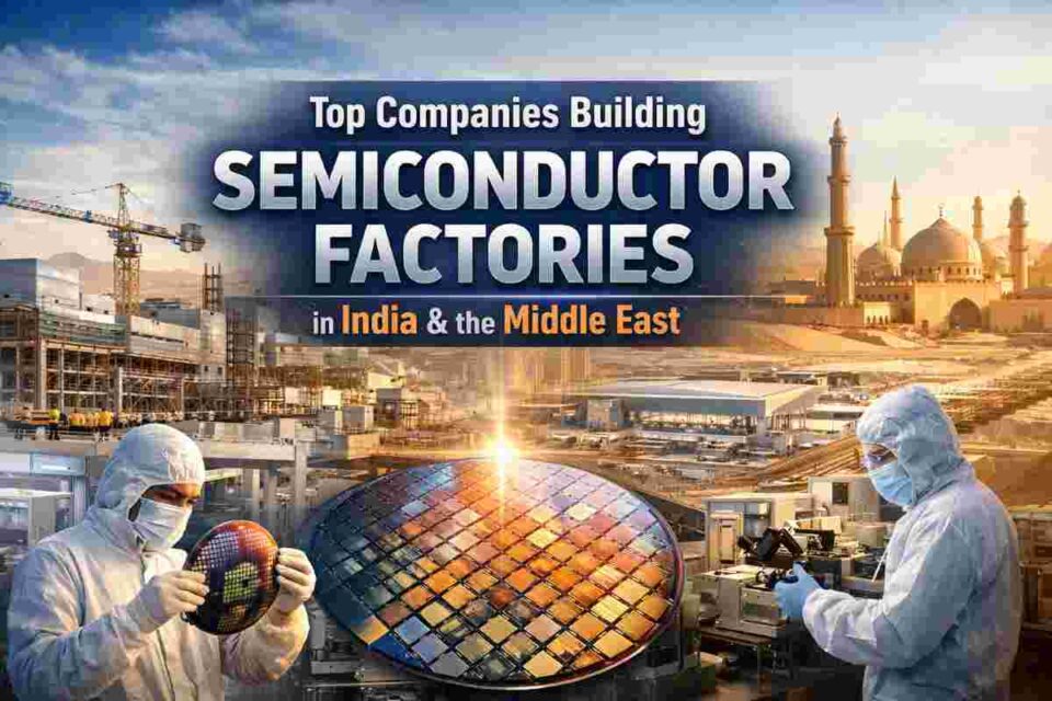
In this listicle, we cover the 11 most significant companies actively building or funding semiconductor fabrication plants in India and the Middle East as of 2026 — with their official websites, investment figures, project status, and what each means for construction professionals.
📋 In This Article
- Why India and the Middle East Are the New Chip Frontier
- Companies Building Semiconductor Fabs in India (#1–#5)
- Companies Building Semiconductor Fabs in the Middle East (#6–#11)
- Side-by-Side Comparison: All 11 Companies
- Career Opportunities for Construction Engineers
- Skills, Certifications, and Salary Outlook
- What’s Coming: 2026 and Beyond
- FAQs
Why India and the Middle East Are the New Semiconductor Frontier
For most of the 21st century, chip manufacturing was a Taiwan–South Korea–USA triangle. That model began to unravel after 2020 for three converging reasons:
- The pandemic chip shortage paralysed global automotive, electronics, and medical device production, exposing how fragile geographic concentration had become.
- US–China decoupling triggered sweeping export controls that forced chipmakers to reconfigure supply chains away from China-dependent nodes.
- The CHIPS Act effect — the US government’s USD 52 billion chip investment — catalysed competing national strategies in India, UAE, Saudi Arabia, and Israel.
India responded with the ₹76,000 crore India Semiconductor Mission (ISM). The UAE launched its National Advanced Technology Strategy (NATS). Saudi Arabia embedded chips into the core of Vision 2030. Israel expanded its relationship with Intel into a USD 25 billion commitment.
The result: a construction pipeline that did not exist five years ago is now one of the most active in the world.
🇮🇳 Companies Building Semiconductor Factories in India
1. Tata Electronics Private Limited (TEPL) — India’s Largest Fab
| 📍 Location | Dholera Special Investment Region, Gujarat, India |
| 💰 Investment | ~₹91,000 crore (approx. USD 11 billion) |
| 🏗️ Status (2026) | Under active construction and infrastructure build-out |
| 🔗 Official Website | www.tataelectronics.com |
| 🤝 Partner | PSMC – Powerchip Semiconductor Manufacturing Corp, Taiwan |
| ⚙️ Technology Node | 28nm (automotive, industrial, consumer electronics) |
Tata Electronics is leading India’s most ambitious semiconductor bet. The Dholera fab — developed in partnership with Taiwan’s Powerchip Semiconductor Manufacturing Corp (PSMC) — will be India’s first commercial front-end semiconductor wafer fab at scale. At 28nm, it targets the massive global market for automotive chips, industrial controllers, and consumer electronics — not bleeding-edge AI chips, but chips that the world needs in enormous quantities.
The Dholera Special Investment Region itself is a greenfield smart city being built from scratch, which means the construction challenge is compounded: roads, utilities, water infrastructure, and worker accommodation all need to be built alongside the fab. Tata Projects (the construction arm of the Tata Group) is handling key EPC packages.
For construction professionals: This is the largest single fab construction programme in India’s history and one of the biggest construction projects on the subcontinent. Civil, structural, MEP, cleanroom, and project management professionals are in active demand across multiple contractor tiers.
2. Micron Technology — India’s First Major Foreign Fab Investor
| 📍 Location | Sanand, Gujarat, India |
| 💰 Investment | USD 2.75 billion (with government incentive support) |
| 🏗️ Status (2026) | Advanced construction; operations commencing |
| 🔗 Official Website | www.micron.com |
| 🏭 Facility Type | ATMP – Assembly, Testing, Marking, and Packaging |
| 🎯 Products | DRAM and NAND flash memory packaging |
Micron Technology — one of the world’s three major DRAM and NAND flash chip makers — broke ground on its Sanand ATMP facility in 2023, making it India’s first large-scale foreign semiconductor manufacturing investment. While an ATMP (packaging) facility rather than a front-end wafer fab, the construction complexity is immense.
The Sanand plant requires ESD-controlled flooring, precision cleanroom environments, specialist HVAC systems, high-density electrical distribution, and chemical handling infrastructure. Multiple Indian and international construction firms are engaged across the project packages.
Why this matters: Micron’s Sanand facility is a proof of concept for India’s ability to attract and deliver semiconductor manufacturing at international standard. Its success will directly accelerate further foreign fab investment decisions.
3. CG Power and Industrial Solutions — Automotive Chip Localisation
| 📍 Location | Sanand, Gujarat, India |
| 💰 Investment | ~₹7,600 crore (approx. USD 900 million) |
| 🏗️ Status (2026) | ISM-approved; site preparation and detailed engineering |
| 🔗 Official Website | https://www.cgglobal.com/ |
| 🤝 Partners | Renesas Electronics (Japan), Stars Microelectronics (Thailand) |
| 🏭 Facility Type | OSAT – Outsourced Semiconductor Assembly and Test |
CG Power, a Murugappa Group company and one of India’s most respected electrical equipment manufacturers, is building an OSAT (semiconductor assembly and testing) facility in Sanand in partnership with Japan’s Renesas Electronics and Thailand’s Stars Microelectronics. The facility will produce automotive-grade and industrial semiconductors — critical for India’s booming EV and automotive sector.
Renesas is a global leader in microcontrollers for vehicles, making this partnership strategically important for India’s domestic automotive supply chain. The construction programme includes specialist cleanroom fit-out, precision mechanical systems, and chemical handling infrastructure.
🔗 Partner website: www.renesas.com (Renesas Electronics)
4. Kaynes Semicon — Compound Semiconductor Specialist
| 📍 Location | Sanand, Gujarat, India |
| 💰 Investment | ~₹3,300 crore (approx. USD 400 million) |
| 🏗️ Status (2026) | ISM-approved; site development in progress |
| 🔗 Official Website | www.kaynessemicon.com |
| 🏭 Facility Type | OSAT + Compound Semiconductors |
| 🎯 Specialisation | SiC, GaN chips for power electronics and EV |
Kaynes Semicon — the semiconductor unit of Kaynes Technology, one of India’s leading electronics manufacturing services companies — focuses on compound semiconductors: Silicon Carbide (SiC) and Gallium Nitride (GaN) chips used in power electronics, electric vehicles, and high-frequency communications. This niche makes Kaynes Semicon one of the more technically distinctive projects in India’s fab pipeline.
Compound semiconductor facilities have unique chemical handling, gas distribution, and material processing requirements that differ from conventional CMOS fab construction — offering a distinct specialisation path for construction engineers looking to build expertise in this area.
5. India Semiconductor Mission (ISM) — The Government Engine Behind It All
| 📍 Jurisdiction | India (MeitY — Ministry of Electronics and IT) |
| 💰 Total Incentive Fund | ₹76,000 crore (~USD 9.4 billion) |
| 🏗️ Projects Approved | 5+ projects across fab, OSAT, and ATMP categories |
| 🔗 Official Website | www.ism.gov.in |
| 🎯 Goal | USD 100 billion domestic semiconductor economy by 2030 |
While ISM is a government programme rather than a company, it is the single most important driver of semiconductor construction activity in India and deserves its place on this list. Every fab project in India is either directly approved through ISM or has been structured to qualify for ISM incentives.
ISM provides up to 50% fiscal support for front-end fab projects and up to 30% for OSAT/ATMP projects — making India one of the most incentive-rich environments for semiconductor capital deployment in the world. New application rounds through 2026 are expected to bring additional international chipmakers into India’s construction pipeline.
For construction firms: Monitor ISM approvals closely — each approval triggers a multi-year EPC procurement cycle worth hundreds of millions to billions of dollars.
🇦🇪 🇸🇦 🇮🇱 Companies Building Semiconductor Factories in the Middle East
6. Intel Corporation — The Middle East’s Biggest Active Fab Build
| 📍 Location | Kiryat Gat, Israel (Fab 38 expansion) |
| 💰 Investment | USD 25 billion committed |
| 🏗️ Status (2026) | Active multi-phase construction |
| 🔗 Official Website | www.intel.com |
| 🏭 Facility Type | Front-end wafer fab (advanced technology nodes) |
| 👷 Construction Jobs | 10,000+ construction-phase positions estimated |
Intel’s Kiryat Gat expansion in southern Israel is, unambiguously, the largest semiconductor construction project in the entire Middle East region — and one of the five largest in the world. With USD 25 billion committed, this multi-phase expansion is adding cutting-edge fabrication capacity for Intel’s advanced chips, including processors for AI and cloud computing workloads.
Intel has operated in Israel since 1974 and employs over 12,000 people in the country. The Kiryat Gat facility has been expanding continuously and remains Intel’s most strategically important fab outside the United States. Despite regional geopolitical tensions in 2024–2025, Intel has maintained its commitment to Israel as a long-term manufacturing hub.
For construction professionals: Israel-based construction firms and international subcontractors working on the Kiryat Gat expansion are handling some of the most technically demanding cleanroom, MEP, and structural work in the world. Salaries and project complexity at this level represent the top tier of fab construction careers.
7. GlobalFoundries — The UAE’s Homegrown Chip Champion
| 📍 Headquarters | USA (majority-owned by Mubadala, Abu Dhabi) |
| 💰 Mubadala Stake | ~85% ownership through Mubadala Investment Company |
| 🏗️ UAE Status | Strategic manufacturing evaluation; MoUs in place |
| 🔗 Official Website | www.globalfoundries.com |
| 🏭 Current Fabs | USA (New York, Vermont), Germany, Singapore |
| 🤝 UAE Owner | www.mubadala.com (Mubadala Investment Company) |
GlobalFoundries is the world’s fourth-largest contract chipmaker and holds a unique position in the Middle East: it is majority-owned by Abu Dhabi’s Mubadala Investment Company, giving the UAE a direct stake in a Tier-1 global semiconductor manufacturer. This ownership structure makes GF the most likely vehicle through which the UAE will establish domestic chip manufacturing capability.
While GF currently does not manufacture in the UAE, the strategic logic for a UAE fab — leveraging sovereign ownership, clean energy, geographic positioning, and capital — is compelling. Analysts widely expect a UAE fab announcement within the next 3–5 years. When it comes, it will be one of the most significant construction events in Middle East industrial history.
GF’s existing fabs in New York (Fab 8) and Germany (Fab 1) give experienced construction professionals a clear pathway: gaining fab experience on GF’s existing builds creates a direct pipeline to any UAE facility that follows.
8. TSMC — The World’s Most Powerful Chipmaker Eyes the Gulf
| 📍 Reported Interest | UAE (Abu Dhabi) — in advanced strategic discussions |
| 💰 Potential Scale | Multi-billion dollar fab (no confirmed figure) |
| 🏗️ Status (2026) | No construction confirmed; diplomatic negotiations ongoing |
| 🔗 Official Website | www.tsmc.com |
| 🏭 Technology | Leading-edge nodes (2nm–5nm in existing fabs) |
| 🌍 Existing Expansion | Arizona (USA), Japan (熊本), Germany (Dresden) |
Taiwan Semiconductor Manufacturing Company — which makes chips for Apple, NVIDIA, AMD, and virtually every major tech brand — is in reported strategic discussions with UAE leadership about a potential manufacturing presence in Abu Dhabi. No construction announcement has been confirmed as of early 2026, but the discussions represent the highest-stakes semiconductor deal in Middle East history.
The UAE’s appeal to TSMC rests on several pillars: vast sovereign capital, ambitions for clean energy-powered manufacturing, a stable geopolitical position outside the Taiwan Strait risk zone, and proximity to European and African markets. Any confirmed TSMC commitment would trigger an immediate, massive EPC procurement cycle across civil, structural, cleanroom, and MEP disciplines.
What to watch: TSMC’s current global expansion (Arizona, Japan, Germany) is consuming enormous construction capacity. A UAE facility would likely be confirmed for post-2027 delivery — giving construction firms time to position themselves now.
9. G42 (UAE) — Building the Semiconductor Ecosystem, Not Just One Fab
| 📍 Location | Abu Dhabi, UAE (multiple sites) |
| 💰 AUM / Investments | USD 10+ billion across AI and deep-tech infrastructure |
| 🏗️ Status (2026) | Actively constructing AI data centres and chip-adjacent facilities |
| 🔗 Official Website | www.g42.ai |
| 🤝 Key Partners | Microsoft (USD 1.5B investment), OpenAI, Cerebras |
| 🎯 Relevance | Semiconductor ecosystem builder: data centres, chip design, testing |
G42 is Abu Dhabi’s leading AI and advanced technology holding company, operating at the intersection of artificial intelligence, cloud infrastructure, and semiconductor strategy. While G42 is not a fab operator, it is constructing the demand-side infrastructure that justifies fab investment: hyperscale AI data centres, chip design centres, and advanced materials research facilities — all of which require precision construction work.
G42’s USD 1.5 billion partnership with Microsoft includes commitments to AI infrastructure deployment in the UAE that will consume chips at massive scale. This demand creates the business case for domestic chip manufacturing — which is precisely why G42’s construction pipeline is so relevant to the semiconductor story.
Masdar City, G42’s preferred UAE technology hub, is actively building out precision facilities — creating immediate opportunities for MEP engineers, cleanroom specialists, and construction project managers.
10. Saudi Aramco Ventures + PIF — The Kingdom’s USD 40B+ Tech Push
| 📍 Location | Saudi Arabia (Riyadh, NEOM, and industrial zones) |
| 💰 Technology Fund | Part of PIF’s USD 40+ billion technology investment mandate |
| 🏗️ Status (2026) | Active ecosystem development; fab announcement expected by 2027 |
| 🔗 Saudi PIF Website | www.pif.gov.sa |
| 🔗 Saudi Aramco Ventures | wa’ed (Aramco Ventures) |
| 🏭 Bodies Involved | KACST, NEOM, NIDLP, Saudi Aramco |
Saudi Arabia has embedded semiconductor production into the core of its Vision 2030 economic diversification programme. The Public Investment Fund (PIF) — managing over USD 750 billion in assets — has designated advanced technology, including chip manufacturing, as a priority investment sector. KACST (King Abdulaziz City for Science and Technology) is leading international partnerships in chip design and compound semiconductor research.
NEOM’s “Aqaba” advanced manufacturing zone explicitly includes semiconductor facilities in its long-term infrastructure design. With NEOM itself representing a USD 500 billion construction programme, the semiconductor component is a significant but relatively small slice of an already enormous project pipeline.
Saudi Arabia is expected to make a formal large-scale semiconductor investment announcement before 2027, likely involving one or more Tier-1 Asian chipmakers seeking Gulf manufacturing diversity. When it lands, it will be the largest new fab programme in the broader region since Intel’s Israeli commitments.
11. Applied Materials & ASML — The Equipment Giants Shaping Regional Construction
| 📍 Presence | Israel, UAE, India (offices and R&D collaborations) |
| 🔗 Applied Materials | www.appliedmaterials.com |
| 🔗 ASML | www.asml.com |
| 🎯 Role | Semiconductor equipment supply and installation infrastructure |
| 💡 Why They Matter | No fab can be built or operated without their equipment |
Applied Materials (USA) and ASML (Netherlands) are the two most critical equipment suppliers to the global semiconductor industry. Applied Materials makes the deposition, etching, and inspection tools that process silicon wafers. ASML makes the lithography systems — including the EUV machines costing USD 150–350 million each — that print circuit patterns onto chips. Without them, no fab can operate.
Both companies have significant and growing presences in the Middle East and India:
- Applied Materials has R&D collaboration centres and equipment service infrastructure in Israel, and is establishing engineering support presence in India to support the Tata and Micron projects.
- ASML actively supplies equipment to regional chip packaging facilities and is a key player in the India and UAE semiconductor ecosystem discussions.
Their presence creates downstream construction demand — every equipment installation in a new fab requires specialist foundation work, utility connections, cleanroom fit-out, and MEP infrastructure. Applied Materials and ASML installations are among the highest-precision construction tasks in the industry.
All 11 Companies at a Glance — Side-by-Side Comparison
| # | Company | Country | Investment (USD) | Type | Status 2026 | Website |
|---|---|---|---|---|---|---|
| 1 | Tata Electronics (TEPL) | 🇮🇳 India | ~USD 11B | Front-end Fab (28nm) | 🟡 Under construction | tataelectronics.com |
| 2 | Micron Technology | 🇮🇳 India | USD 2.75B | ATMP | 🟢 Advanced / commissioning | micron.com |
| 3 | CG Power + Renesas | 🇮🇳 India | ~USD 900M | OSAT | 🟡 Site preparation | cgpower.com |
| 4 | Kaynes Semicon | 🇮🇳 India | ~USD 400M | OSAT + Compound Semi | 🟡 ISM-approved / planning | kaynes.in |
| 5 | India Semiconductor Mission | 🇮🇳 India | USD 9.4B incentives | Govt. Programme | 🟢 Active — new rounds open | semiconductors.india.gov.in |
| 6 | Intel Corporation | 🇮🇱 Israel | USD 25B | Advanced Front-end Fab | 🟢 Active construction | intel.com |
| 7 | GlobalFoundries / Mubadala | 🇦🇪 UAE | TBD | Fab (proposed) | 🟠 Strategic evaluation | globalfoundries.com |
| 8 | TSMC | 🇦🇪 UAE | TBD | Fab (discussions) | 🟠 Diplomatic talks | tsmc.com |
| 9 | G42 | 🇦🇪 UAE | USD 10B+ | Ecosystem / AI infra | 🟢 Active builds | g42.ai |
| 10 | Saudi PIF / Aramco / KACST | 🇸🇦 Saudi Arabia | USD 40B+ tech mandate | Fab + ecosystem | 🟡 Ecosystem building | pif.gov.sa |
| 11 | Applied Materials + ASML | 🌍 Regional | N/A (equipment supply) | Equipment + infra | 🟢 Active regional presence | appliedmaterials.com |
🟢 Active | 🟡 In progress / planning | 🟠 Strategic discussions | 🔴 Restructuring
Career Opportunities for Construction Professionals in Semiconductor Fab Projects
Semiconductor fab construction sits at the absolute top tier of technical complexity in the construction industry — combining hospital-grade cleanroom standards, industrial plant chemical systems, and data centre-level power infrastructure, all in one building. This complexity translates directly into premium compensation.
Most In-Demand Roles Across Active Fab Projects (2026)
| Role | Key Skills Required | Experience Level |
|---|---|---|
| Civil / Structural Engineer | Vibration isolation, heavy foundations | 5–15 years |
| HVAC / Cleanroom Engineer | ISO 14644, SEMI standards, airflow design | 7–15 years |
| Electrical Engineer (HV) | Substations, UPS, N+2 redundancy design | 8–15 years |
| Piping Engineer (UPW / Chemical) | UPW systems, process gas, chemical distribution | 6–12 years |
| Planning Engineer (P6) | Primavera P6, complex multi-phase scheduling | 5–12 years |
| BIM Coordinator | Revit, Navisworks, clash detection | 4–10 years |
| Project Manager | PMP, multi-discipline EPC delivery | 10–20 years |
| Commissioning Manager | FAT/SAT, system integration, validation | 10–18 years |
If you are looking to transition into high-tech construction, start by exploring our guide on moving from civil engineering to project management and our comprehensive overview of data centre construction careers — which share significant technical overlap with fab builds.
Use the AI-powered Career Planner and Resume Lab at ConstructionCareerHub.com to tailor your profile for semiconductor or high-tech construction roles.
Skills, Certifications, and Salary Outlook for Fab Construction Roles
Must-Have Certifications
- ✅ PMP — Near-mandatory for project management roles on large EPC fab programmes
- ✅ NEBOSH IGC / International Diploma — Required for safety-critical chemical and cleanroom environments
- ✅ Primavera P6 Certified User — Standard for planning and scheduling roles
- ✅ Autodesk Revit / Navisworks (BIM) — Increasingly mandatory on large fab coordination teams
- ✅ LEED AP or equivalent — Growing requirement as semiconductor companies pursue sustainability targets
Explore the full list in our most valuable construction certifications guide and understand how a BIM specialisation opens doors to fab and data centre projects.
Salary Outlook — India vs Middle East
| Role | India (LPA) | Middle East (USD/month) |
|---|---|---|
| Civil / MEP Engineer (5–10 yrs) | ₹12–22 LPA | USD 3,000–5,500 |
| Cleanroom HVAC Engineer | ₹18–30 LPA | USD 5,000–8,000 |
| Planning Engineer (Primavera) | ₹14–24 LPA | USD 4,500–7,000 |
| Project Manager | ₹25–55 LPA | USD 8,000–14,000 |
| Construction / Programme Director | ₹60–100+ LPA | USD 15,000–25,000 |
Middle East packages typically include housing allowance, annual flights, and comprehensive health insurance — significantly enhancing total compensation beyond the base salary. See our detailed construction salary guide for Gulf countries for a full breakdown by role and location.
Use the free Salary Calculator at ConstructionCareerHub.com to benchmark your current package and understand what to negotiate for on a semiconductor project.
Recommended Courses for Fab-Ready Construction Professionals
- 🎓 Project Management Principles and Practices — Coursera (UC Irvine)
- 🎓 Autodesk Revit for Structural Design
- 🎓 Primavera P6 for Construction Project Scheduling — Udemy
Future Outlook: What’s Coming in 2026 and Beyond
India’s Semiconductor Construction Pipeline to 2030
- Government target: USD 100 billion domestic semiconductor economy by 2030 — requiring 4–6 additional fab or OSAT projects beyond those already announced
- New ISM rounds expected through 2026–2027 — bringing fresh international chipmakers into India’s pipeline
- State competition intensifying: Karnataka, Tamil Nadu, Telangana, and Uttar Pradesh are developing dedicated semiconductor industrial parks with supporting infrastructure
- India’s defence electronics push (radar, guidance, communications chips) will drive additional military-grade fab investment outside the civilian ISM framework
Middle East’s Semiconductor Construction Pipeline to 2030
- UAE’s National Advanced Technology Strategy targets self-sufficiency in chip design and packaging by 2031 — a GlobalFoundries UAE facility announcement is widely anticipated before 2030
- Saudi Arabia’s PIF expected to announce a major semiconductor investment before 2027
- Intel Kiryat Gat expansion will remain the region’s largest active fab build through at least 2028
- Mubadala’s ownership of GlobalFoundries positions the Gulf for a potential direct entry into front-end manufacturing at a scale no other region outside East Asia and the US can match
For construction professionals, this represents a sustained 7–10 year project pipeline — with premium compensation, transferable international experience, and strong career trajectory. Explore semiconductor construction jobs on ConstructionPlacements.com and discover the broader universe of hidden construction careers that pay more than engineering.
Prepare for interviews with EPC firms active on fab projects using the Interview Copilot at ConstructionCareerHub.com — with role-specific technical Q&A practice built for construction professionals.
Also check international construction opportunities alongside semiconductor projects: construction jobs in Canada and construction jobs in Australia where large-scale infrastructure projects of comparable complexity are also active in 2026.
Frequently Asked Questions
Which companies are building semiconductor factories in India in 2026?
The main companies building semiconductor factories in India in 2026 are Tata Electronics (with PSMC, in Dholera), Micron Technology (ATMP facility in Sanand), CG Power (with Renesas, OSAT in Sanand), and Kaynes Semicon (compound semiconductor OSAT in Sanand). The Indian government’s India Semiconductor Mission (ISM) is the central driver of all these investments, providing up to 50% fiscal support.
Which is the largest semiconductor factory project in the Middle East?
Intel’s Kiryat Gat fab expansion in Israel is the largest semiconductor construction project in the broader Middle East, with a committed investment of approximately USD 25 billion. In the Gulf specifically, the UAE — through Mubadala’s majority ownership of GlobalFoundries — is positioned as the most likely location for the region’s first commercial fab in the coming years.
Does the UAE have any semiconductor factories?
As of 2026, the UAE does not yet have an operational front-end semiconductor fab. However, Abu Dhabi’s Mubadala Investment Company owns approximately 85% of GlobalFoundries — one of the world’s largest chipmakers. The UAE’s National Advanced Technology Strategy targets semiconductor manufacturing capability, and an on-shore fab announcement is widely anticipated before 2030. Chip-adjacent facilities, including AI data centres and chip packaging operations, are already active in the UAE.
What is India’s India Semiconductor Mission (ISM)?
The India Semiconductor Mission (ISM) is a ₹76,000 crore (~USD 9.4 billion) government programme under India’s Ministry of Electronics and IT (MeitY), designed to attract domestic and international investment in semiconductor manufacturing. ISM provides fiscal incentives of up to 50% for front-end fab projects and 30% for OSAT/ATMP projects. As of 2026, it has approved projects totalling over USD 15 billion in combined investment.
What construction roles are available in semiconductor fab projects?
Key construction roles in semiconductor fab projects include civil and structural engineers (specialising in vibration isolation), cleanroom HVAC engineers, high-voltage electrical engineers, ultra-pure water (UPW) piping engineers, BIM coordinators, Primavera P6 planning engineers, project managers, and commissioning managers. These roles command a 25–40% salary premium over equivalent positions in general construction.
How does semiconductor fab construction differ from normal industrial construction?
Semiconductor fab construction is significantly more demanding than standard industrial construction. Key differences include: cleanroom environments (ISO Class 3–5) that require micrometer-level air quality control; vibration-isolated structural floors for lithography equipment; ultra-pure water systems purified to near-absolute levels; complex chemical and process gas delivery networks; and N+2 power redundancy systems. Build programmes typically take 3–5 years for a full-scale front-end fab.
Is Saudi Arabia building semiconductor factories?
Saudi Arabia is in the ecosystem-building phase of its semiconductor strategy. The Public Investment Fund (PIF) has designated semiconductors as a priority sector under Vision 2030, and KACST (King Abdulaziz City for Science and Technology) is developing international partnerships in chip design and compound semiconductor research. NEOM’s advanced manufacturing zones include semiconductor facilities in their long-term infrastructure plans. A major fab investment announcement from Saudi Arabia is expected before 2027.
Which EPC companies are working on semiconductor fab construction in India?
Key EPC and construction firms active on India’s fab projects include Tata Projects (Tata Group’s EPC arm), L&T Construction, Shapoorji Pallonji, and international firms including Fluor, Jacobs, and Worley. These firms are handling different packages across civil, structural, MEP, and cleanroom scopes on the Dholera and Sanand fab programmes.
About ConstructionPlacements.com
ConstructionPlacements.com is a global career platform for the construction industry — covering jobs, salaries, certifications, immigration, and career guidance for civil engineers, project managers, MEP engineers, and construction professionals across India, the Gulf, UK, Australia, and North America. For AI-powered career tools, including Resume Lab, Interview Copilot, and Career Planner, visit ConstructionCareerHub.com.